- 您现在的位置:买卖IC网 > Sheet目录983 > HI5828EVAL2 (Intersil)EVALUATION PLATFORM HI5828
�� �
�
�Application� Note� 9855�
�Functional� Descriptions�
�Voltage� Reference�
�The� HI5828� has� an� internal� nominal� 1.2V� voltage� reference�
�with� a� ±� 10ppm/� o� C� drift� coefficient� over� the� industrial�
�temperature� range.� The� REFLO� pin� (18)� selects� the�
�reference.� Access� to� pin� 18� is� provided� through� solder�
�jumpers� J21� and� J22.� These� jumpers� are� labeled� INT� and�
�EXT� for� internal� or� external� reference.� The� REFIO� pin� (17)�
�provides� access� to� the� internal� voltage� reference� and� can� be�
�overdriven� if� the� user� wishes� to� use� an� external� source� for� the�
�reference.� The� internal� reference� was� not� designed� to� drive� an�
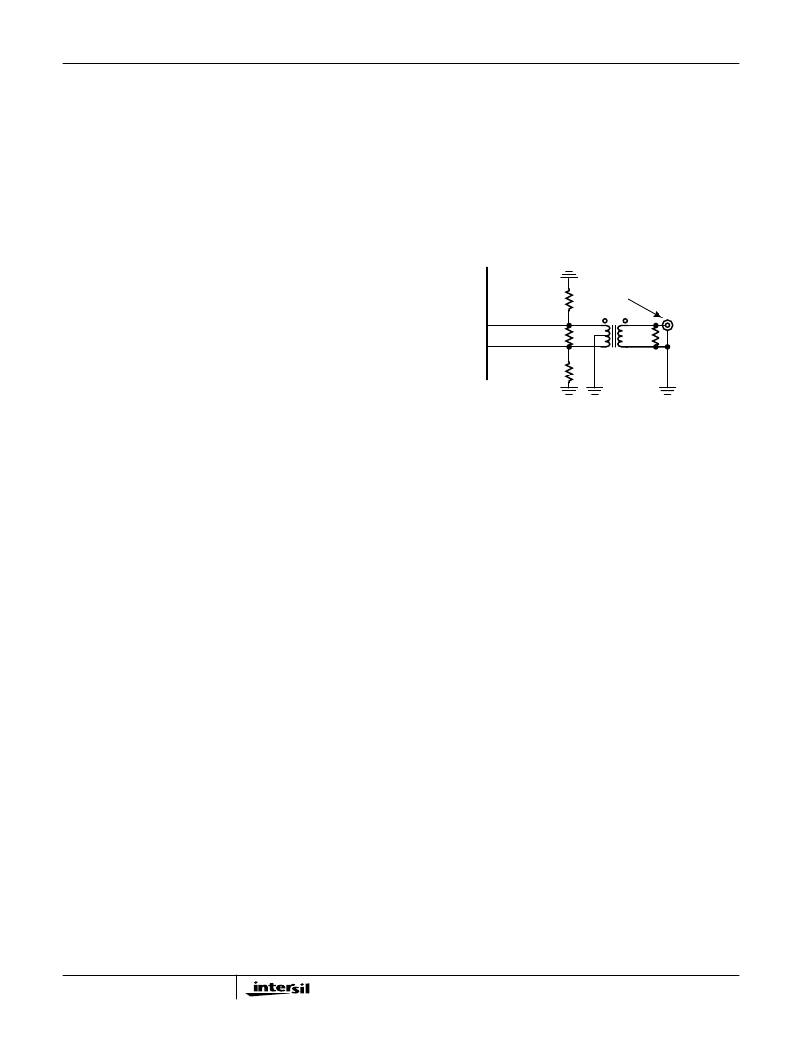
�Transformer� Output�
�The� evaluation� board� is� con?gured� with� a� transformer� output�
�con?guration,� shown� in� Figure� 1.� This� con?guration� was�
�chosen� because� it� provides:� even� harmonic� performance�
�improvement� due� to� the� complimentary� differential� signaling;�
�~12.5� ?� R� EQ� loading� to� each� output� of� the� DAC;� drive�
�impedance� of� 50� ?� for� matching� with� a� spectrum� analyzer;�
�and� 2x� voltage� gain.� The� output� of� this� con?guration� will� be�
�biased� at� zero� volts� and� have� an� amplitude� of� ~500mV�
�(V� OUT� )� when� the� DAC� is� con?gured� to� drive� I� OUTFS� of�
�20mA.�
�external� load.� Notice� that� a� 0.1� μ� F� capacitor� is� placed� as� close�
�as� possible� to� the� REFIO� pin.� This� capacitor� is� necessary� for�
�ensuring� a� noise� free� reference� voltage.�
�If� the� user� wishes� to� use� an� external� reference� voltage,� jumper�
�J23� must� be� in� place� and� an� external� voltage� reference�
�provided� via� J18,� an� SMA� connector� labeled� ‘EXT� REF’.�
�Jumper� J22� must� be� soldered� so� that� pin� 18� (REFLO)� is� tied�
�HI5828�
�PIN� 15� (22)�
�PIN� 16� (21)�
�50� ?�
�IOUTA(QOUTA)�
�100� ?�
�IOUTB(QOUTB)�
�50� ?�
�V� OUT� =� (2� x� I� OUTFS� x� R� EQ� )V�
�50� ?�
�SPECTRUM�
�ANALYZER’S�
�INPUT�
�IMPEDANCE�
�to� a� logic� high� (the� supply� voltage).� The� recommended� limits�
�of� the� external� reference� are� between� 15mV� and� 1.2V.�
�Performance� of� the� converter� can� be� expected� to� decline� as�
�the� reference� voltage� is� reduced� due� to� the� reduction� in� LSB�
�current� size.�
�If� the� user� wishes� to� amplitude� modulate� the� DAC,� the� REFIO�
�pin� can� be� overdriven� with� a� waveform.� The� input� multiplying�
�bandwidth� of� the� REFIO� input� is� approximately� 1.4MHz� when�
�driving� a� 100mV� signal� into� the� REFIO� pin,� biased� at� 0.6V� DC� .�
�The� 3dB� BW� reduces� as� this� amplitude� is� increased.� It� is�
�necessary� that� the� multiplying� signal� be� DC� offset� so� that� the�
�minimum� and� maximum� peaks� are� positive� and� below� 1.2V.�
�The� output� current� of� the� converter,� IOUTA� and� IOUTB,� is� a�
�function� of� the� voltage� reference� used� and� the� value� of� R� SET� ,�
�R43.�
�Output� Current�
�The� output� current� of� the� device� is� set� by� choosing� R� SET�
�and� V� FSADJ� such� that� the� resultant� of� the� following� equation�
�is� less� than� 20mA:�
�I� OUT� =� 32� x� V� FSADJ� /R� SET.�
�REFIO� (Pin� 17)� and� FSADJ� (Pin� 20)� of� the� DAC� are� the�
�inputs� to� an� operational� ampli?er.� The� voltage� at� the� FSADJ�
�pin� (V� FSADJ� )� will� be� approximately� equal� to� the� voltage� at�
�the� REFIO� pin,� which� will� either� be� the� value� of� the� internal�
�or� external� reference.� For� example,� using� the� internal�
�reference� of� (nominal)� 1.2V� and� an� R� SET� value� of� 1.91k� ?�
�results� in� an� I� OUT� of� approximately� 20mA� (maximum�
�allowed).� Choose� the� output� loading� so� that� the� Output�
�Voltage� Compliance� Range� is� not� violated� (-0.3� to� 1.25V).�
�The� output� can� be� con?gured� to� drive� a� load� resistor,� a�
�transformer,� an� operational� ampli?er,� or� any� other� type� of�
�output� con?guration� so� long� as� the� output� voltage�
�compliance� range� and� the� maximum� output� current� are� not�
�violated.�
�3-2�
�FIGURE� 1.�
�Sleep�
�The� converter� can� be� put� into� ‘sleep’� mode� by� connecting� pin�
�9� of� the� DAC� to� either� of� the� converter’s� supply� voltages.� The�
�sleep� pin� has� an� active� pull-down� current,� so� the� pin� can� be�
�left� disconnected� or� be� grounded� for� normal� (awake)�
�operation.� On� the� evaluation� board,� jumper� J15� is� provided�
�for� controlling� the� sleep� pin.� Remove� the� solder� jumper� from�
�J15� for� normal� operation� and� replace� it� for� sleep� mode.�
�Power� Supply(s)� and� Ground(s)�
�The� user� can� operate� from� either� a� single� supply� or� from�
�dual� supplies.� The� supplies� can� be� at� different� voltages.� It� is�
�important� to� note� that� the� digital� inputs� cannot� switch� more�
�than� 0.3V� above� the� digital� supply� voltage.� The� evaluation�
�board� contains� two� power� supply� connections,� (analog)�
�AVDD� and� (digital)� DVDD,� each� with� their� own� ground� wire.�
�Dual� ground� and� power� planes� is� the� recommended�
�con?guration,� with� the� ground� planes� connected� at� a� single�
�point� (J7� on� the� evaluation� board).� Error� on� the� board:� the�
�labels� for� DGND� and� AGND� are� swapped.� The� DGND� label�
�is� next� to� the� analog� ground� connection� and� the� AGND� label�
�is� next� to� the� digital� ground� connection.�
�Digital� Inputs�
�The� DAC� is� designed� to� accept� CMOS� inputs.� The� switching�
�voltage� is� approximately� 1/2� of� the� digital� power� supply�
�voltage,� so� reducing� the� power� supply� can� make� the� DAC�
�compatible� to� smaller� levels.� The� digital� inputs� (data� and�
�clock)� cannot� go� +0.3V� higher� than� the� digital� supply�
�voltage,� else� diode� ESD� protection� can� begin� to� turn� on� and�
�performance� could� be� degraded.� The� clock� source� can� be� a�
�sine� wave,� with� some� degradation� in� performance� possible.�
�The� recommended� clock� is� a� square� wave.�
�发布紧急采购,3分钟左右您将得到回复。
相关PDF资料
HI5960SOICEVAL1
EVALUATION PLATFORM SOIC HI5960
HI7188EVAL
EVALUATION PLATFORM HI7188
HI7190EVAL
EVALUATION PLATFORM HI7190
HJ4-L-DC12V
RELAY GEN PURPOSE 4PDT 5A 12V
HL2-HP-AC100V-F
RELAY GEN PURPOSE DPDT 10A 100V
HLM01510Z16K50JJ
RES 16.5K OHM 15W 5% WW
HMC1043-DEMO
DEMONSTRATION BOARD FOR HMC1043
20021311-00034T1LF
集管和线壳 RCPT VT TH
相关代理商/技术参数
HI5828IN
功能描述:DAC DUAL 12BIT 130MHZ 48-LQFP RoHS:否 类别:集成电路 (IC) >> 数据采集 - 数模转换器 系列:- 标准包装:2,400 系列:- 设置时间:- 位数:18 数据接口:串行 转换器数目:3 电压电源:模拟和数字 功率耗散(最大):- 工作温度:-40°C ~ 85°C 安装类型:表面贴装 封装/外壳:36-TFBGA 供应商设备封装:36-TFBGA 包装:带卷 (TR) 输出数目和类型:* 采样率(每秒):*
HI5860
制造商:INTERSIL 制造商全称:Intersil Corporation 功能描述:12-Bit, 125MSPS, CommLinkTM High Speed D/A Converter
HI5860 WAF
制造商:Intersil Corporation 功能描述:
HI5860_05
制造商:INTERSIL 制造商全称:Intersil Corporation 功能描述:12-Bit, 130MSPS, High Speed D/A Converter
HI5860_08
制造商:INTERSIL 制造商全称:Intersil Corporation 功能描述:12-Bit, 130MSPS, High Speed D/A Converter
HI5860IA
功能描述:CONV D/A 12BIT 130MSPS 28-TSSOP RoHS:否 类别:集成电路 (IC) >> 数据采集 - 数模转换器 系列:- 标准包装:2,400 系列:- 设置时间:- 位数:18 数据接口:串行 转换器数目:3 电压电源:模拟和数字 功率耗散(最大):- 工作温度:-40°C ~ 85°C 安装类型:表面贴装 封装/外壳:36-TFBGA 供应商设备封装:36-TFBGA 包装:带卷 (TR) 输出数目和类型:* 采样率(每秒):*
HI5860IA-T
功能描述:CONV D/A 12BIT 130MSPS 28-TSSOP RoHS:否 类别:集成电路 (IC) >> 数据采集 - 数模转换器 系列:- 标准包装:2,400 系列:- 设置时间:- 位数:18 数据接口:串行 转换器数目:3 电压电源:模拟和数字 功率耗散(最大):- 工作温度:-40°C ~ 85°C 安装类型:表面贴装 封装/外壳:36-TFBGA 供应商设备封装:36-TFBGA 包装:带卷 (TR) 输出数目和类型:* 采样率(每秒):*
HI5860IB
功能描述:CONV D/A 12-BIT 130MSPS 28-SOIC RoHS:否 类别:集成电路 (IC) >> 数据采集 - 数模转换器 系列:- 标准包装:2,400 系列:- 设置时间:- 位数:18 数据接口:串行 转换器数目:3 电压电源:模拟和数字 功率耗散(最大):- 工作温度:-40°C ~ 85°C 安装类型:表面贴装 封装/外壳:36-TFBGA 供应商设备封装:36-TFBGA 包装:带卷 (TR) 输出数目和类型:* 采样率(每秒):*